Content
Goal
- VBUS voltage control support for USB OTG Micro connector
- Support for USB charger as power input
- Overvoltage protection for power input jack
This circuit is primary intended to use with our Breakwine project, but we implemented it also in our another projects (e.g. Tiny Rex).
Hardware development
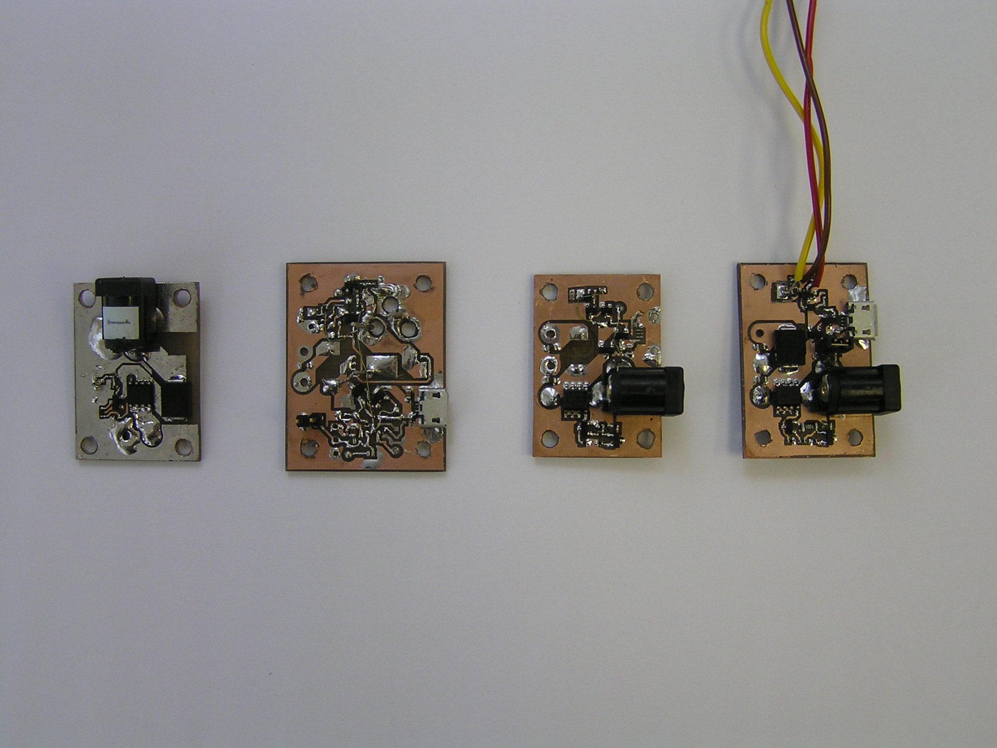
The safest and fastest way to develop a schematic is to use circuit from an existing development board. If special demands are required (e.g. cost or space), sometimes “new” schematic needs to be created. This development can be sometimes tricky. It have to be tested on breakout board or breadboard which consume time.
Overview
The idea how the power input is going to work is shown in picture below. As a power input can be used power jack or USB Micro. Two switches are controlling how the connection is made. From center of switches is taken supply voltage for the whole board (will be called system power).
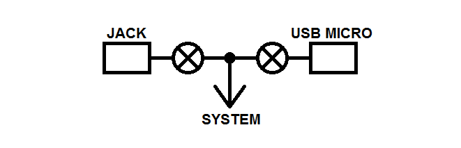
There are more scenarios how the switches should work:
- Board is supplied from power jack. USB charger voltage is disconnected from system power.
- Board is supplied from power jack. USB supply voltage from host connected to USB Micro is disconnected.
- Board is supplied from power jack. Device connected to USB Micro is supplied from our system power.
- Power jack is not plugged in. Board is supplied from USB Charger. (Jumper needs to be fitted to enable it.)
- Power jack is not plugged in. Board will not be supplied from USB Host. (Can be overcome by jumper.)
- Power jack is not plugged in. Board is turn off as the USB micro is connected USB device
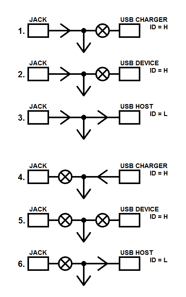
USB function of the board is described by cable which is plugged into the connector. ID signal is tied to low or left floating inside the connector. By this way ID signals are not connected through USB cable and every side of cable can be set for different operation. Two situation can happen:
- When USB A cable is plugged into our connector: We are acting as a host; ID is tied low; on other side a device (peripheral) is connected (e.g. USB stick). We will supply USB voltage.
- When USB B cable is plugged into our connector: We are acting as a device; ID is high (pulled by on board resistor); on other side a host is connected (e.g. PC). USB power is supplied by the other side.
For more info about USB go to Wiki page. Note: In this text the USB function will be described from our board view.
Overvoltage protection
Many of the power supplies IC we use have limited maximum input voltage (in many cases 6V is absolute maximum). A high voltage may easily damaged the board. In most cases this happened when user connect high voltage by mistake. But overvoltage can also occur when some power sources are turn off (see Testing section below).
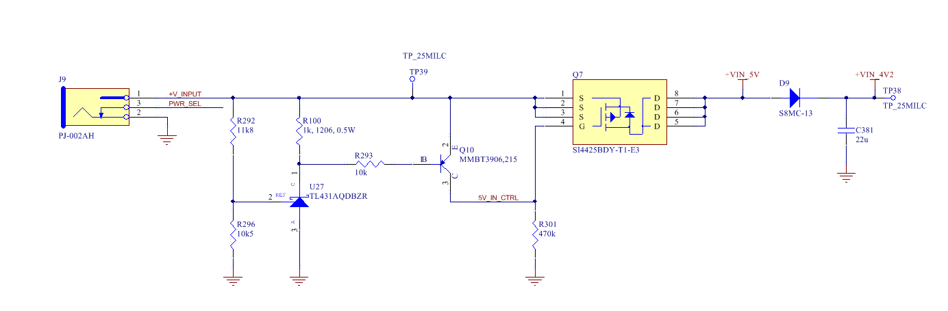
Overvoltage protection is controlled by voltage reference TL431. It uses internal reference 2.495V. When voltage (created by voltage divider R292-R296) on REF pin is lower than this reference, voltage on this pin is tied to +5V_IN. If voltage on REF pin is higher then internal reference, output pin is equal around to 2V. This voltage turn on Q10 which connects source and gate together and turn off the Q7 transistor. By default Q7 is turn on by resistor R301.
Voltage reference divider is turn off the board when voltage is 5.3V or higher (to supports all 5V adapter with 5% accuracy). Important part of design is to select value of resistor R100. It need to be low enough to supply at least 1mA to reference in on state (2V on out pin). Also the voltage drop on R100 needs to be smaller than ~0.5V if off state (in off state reference chip draws 125 uA). To be able to work properly with input voltages up to 24V this resistor need to dissipate enough power (there will be 22V drop on it in this case).
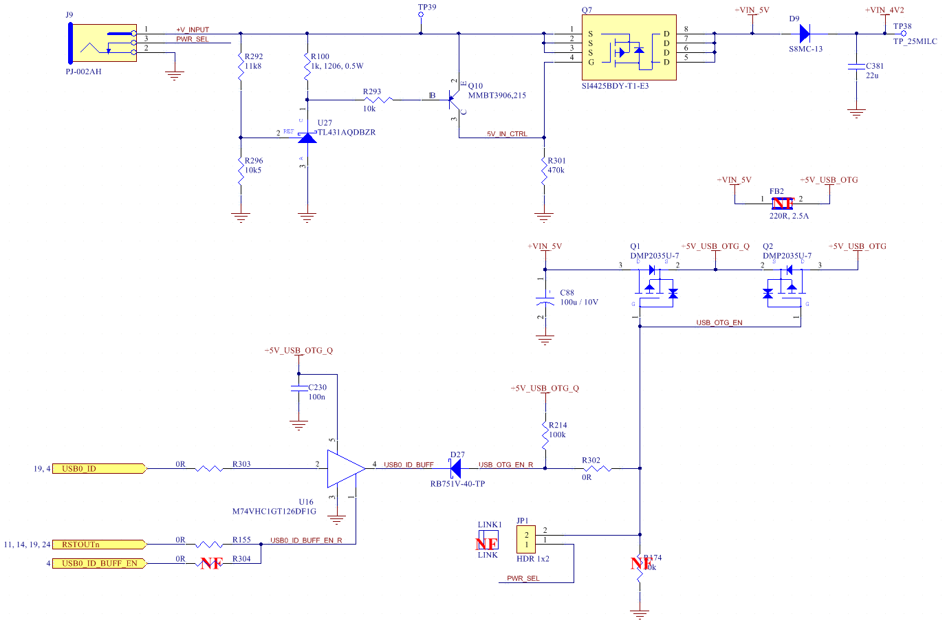
USB Switch
To fully support USB power voltage specification we need to add bidirectional switch. This was created by two P-MOS transistor (because of the protection diodes). This switch is turn off by default (using pullup R214). USB Micro can supply the board only when Power Jack is not plugged in – this is done by using power jack insertion switch. When power jack is unplugged, PWR_SEL is connected to ground. If it is not plugged, PWR_SEL is left unconnected. JP1 jumper connects this switch to control the transistors – only if it is fitted board can be supplied from USB charger.
When state of switch is defined by ID signal (board booted up from power jack), 3-state buffer with Schmitt trigger is used. When board is not fully configured (RSTOUTn is low), buffer is in high impedance state and switch is turn off. To prevent current leaking D27 diode is placed.
The buffer is important to disable ID signal to control the switch when it is not defined (before 3V3 is brought up and system configured). This way we have defined value of this signal in every state.
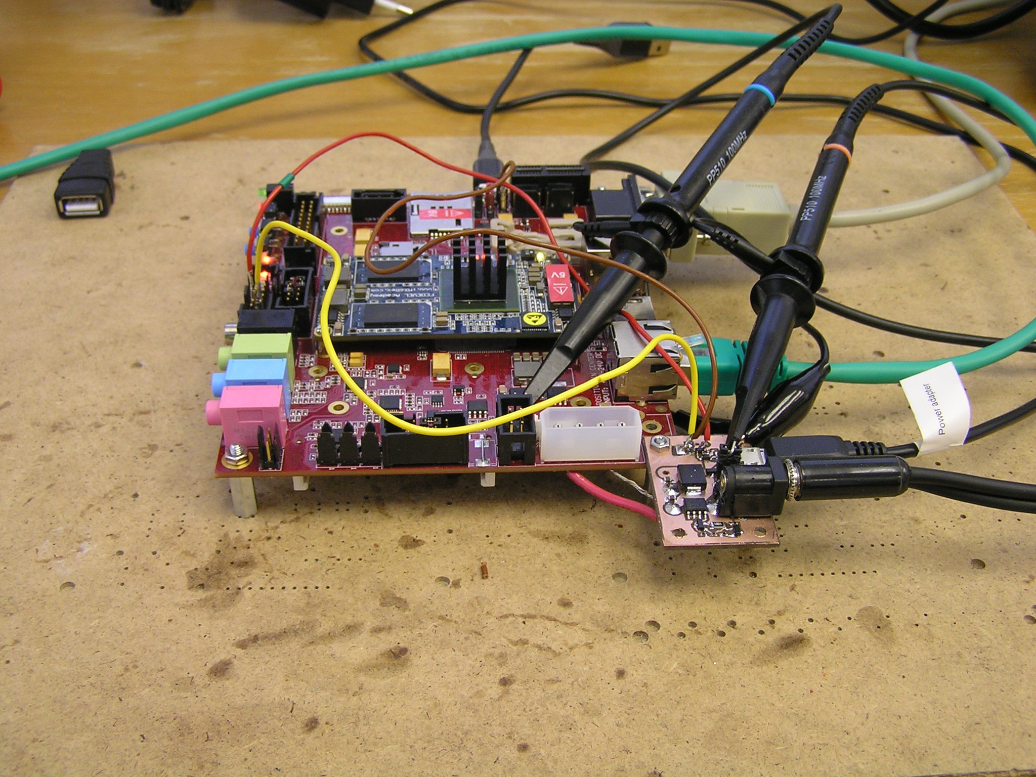
Testing
We tested most of the scenarios with iMX6 Rex 5V version.
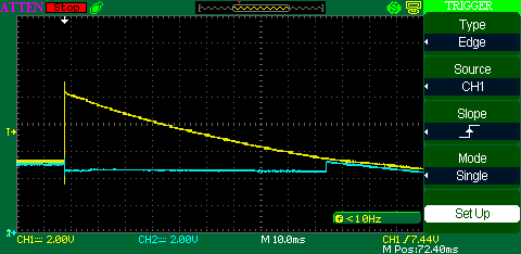
One of the most important measurement was overvoltage protection behaviour. We used power source HY3005-3. When it is turn off it generate high voltage peaks. This peaks can easily damage the board when not suppressed.
Protection is working properly – when voltage is higher than 5.3V it will turn off input voltage. When the voltage went under the threshold, switch is turn on again.
Another important measurement is situation when input leads are swapped – voltage is overpole. In this case input voltage on gate Q7 is higher than on source which turns off the transistor. But through internal diode reverse current can flow. Because of this it is important that the system power is connected with another diode D9.
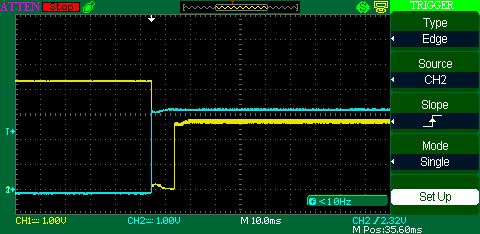
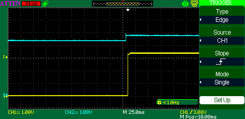
Then we moved to USB switch. From measurement we find out that for a short time after reset the USB switch is incorrectly turn on. You can see this situation on the picture below.
When we plugged power jack with 5 Volts board is being initialized. In this moment USB Switch is turned off by 5V on gates (USB0_ID_BUFF – yellow probe) and RSTOUTn is low (blue probe). When the RSTOUTn goes to high, ID is still low and for this small time the USB switch is opened. After that output of the latch is high with 3V3 level only.
This problem we fixed by placing stronger external pullup to 3V3. This will ensure output of the buffer will be 5V. Also in moment when board is configuring and all power rails is valid, resistor pulled up ID to high. When reset goes high ID is in default state. To be sure that buffer will not be enabled before ID is valid, se add option to control the buffer with GPIO pin.
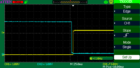
You can see little jump on USB0_ID_BUFF when reset is triggered. This is because buffer starts working and has higher voltage than from pullup (there is 2 diodes Q1-D27 voltage drop) .
When Jack is plugged and USB A-cable is plugged – ID is low you can see before the reset supply voltage is on.
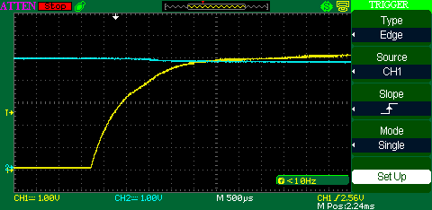
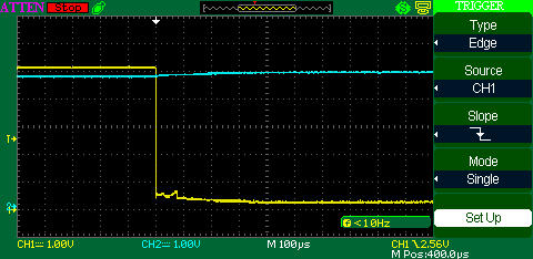
Next testing what we have tried was changing the power connector when board is running. When board was run from USB charger and we plugged the power jack. We will test if the board will not reset or if the 2 plugged voltages will not damage anything. Also on high load (stressapptest running) board was not reseted in any case. Voltage on USB charger was 5.18V and on power jack 4.96V to be able to see the change. As trigger signal we used power jack insertion switch.
Another test what we have done was testing if maximum voltage on power jack (24V) will not damage anything and create voltage leak to system. After 1 whole day running at 22V there was no voltage on system site.
Next test was constantly turning on and off the board to see if the circuit can really protect power supplies on the board. This test was done with iMX6 Tiny Rex board.
As you can see this kind of development and testing can be quite time consuming. Sometimes more version are needed to take this custom circuit to final revision. Final breakout is on the right.