
Content
Overview
The main advantage of this solution is the number of components needed and thus a board cost. On the other hand, before we will use this IC, we need to configure it first . Because of our special requirements, we could not use any of the offered pre-programmed version for this PMIC (we used a NP version). The programming procedure affects the One Time Programmable (OTP) registers. This PMIC series offer also an option to try it without permanent programming - Try Before Buy mode. For more info about the procedure have a look at the product datasheet (original document here) and at the programming application note (or here).Testing with development board
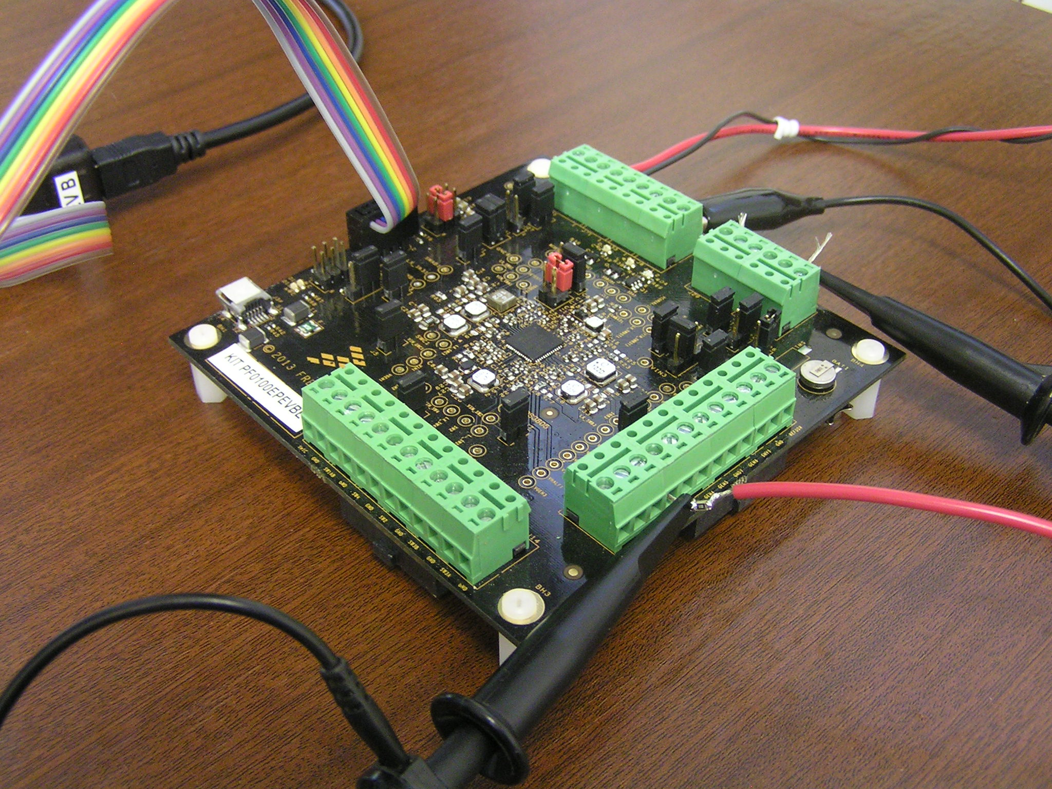
Before we will program the OpenRex board, we will test the configuration using MMPF0100 evaluation board. This board provides all the PMIC options and capabilities. We also test configuring PMIC with PF Series Programmer. The procedure described below is slightly more complicated than the recommended programming steps, but this way we will emulate how the OpenRex board will be used.Programming procedure with the development board:
1. Download and install the latest software for the PF family (you may need to sign up at the NXP site). Note: From version 4.1 and above, you don't need to download any other software and drivers (as described in datasheet).
2. Open PF_Series_HID.application and connect PF Series Programmer with PC using USB Mini cable.
3. Check development board jumpers. Use default jumper configuration as described in evaluation kit datasheet with these exceptions:
- OTP programming voltage jumper J17: fit in 3-4 position (start-up from TBBOTP registers)
- 3V3 voltage selection jumper J46: when programming use 1-2 position
5. Connect programmer together with evaluation board header J36.
6. Enable Target and scan for the devices in the application. At this point you should see these messages in the log area:
Target = PF-Programmer
Device Found
3.3V Supply Enabled
Target Enabled
Device with address [0x08] available
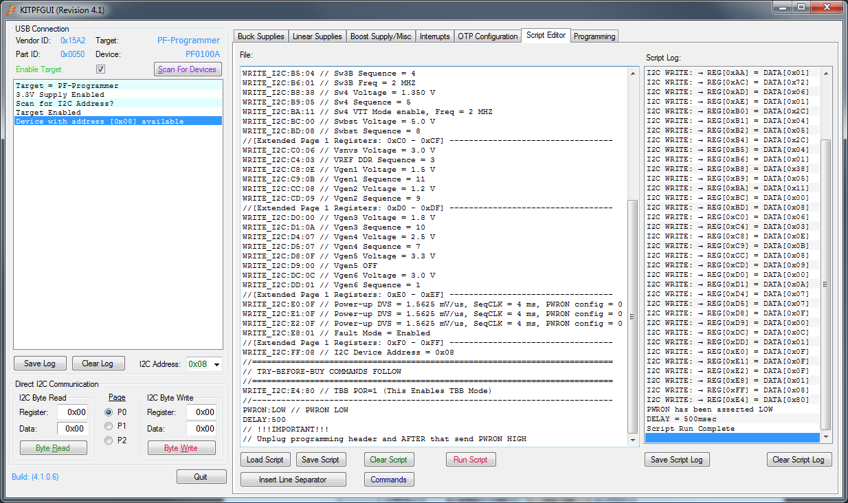
7. Go to script Editor tab and Copy there our Try before buy script.
8. Run the script. At this point your GUI should look something like this.
9. Fit link J26 (Tie PWRON to low)
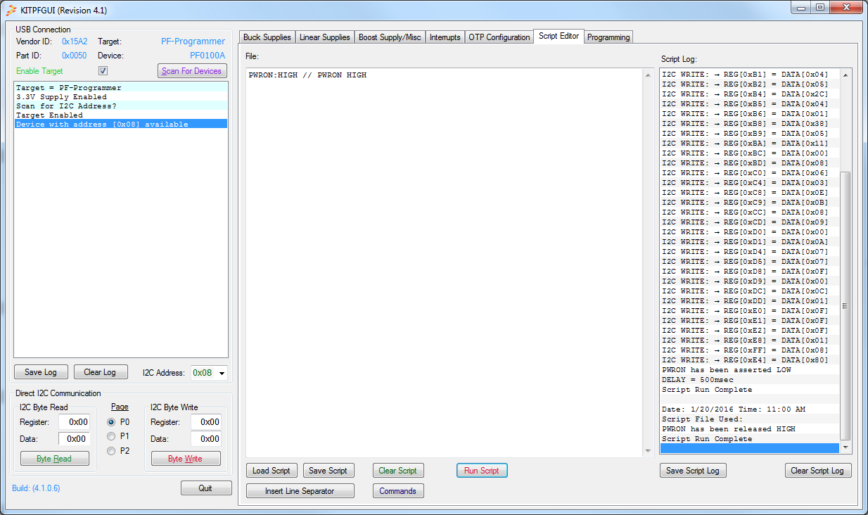
10. Send command through Script editor (clear existing first) to put PWRON high (send PWRON:HIGH).
11. Change link position on jumper J46 from 1-2 to 3-4 (to switch the 3V3 source voltage).
12. Remove programming header.
13. Release PWRON signal (remove the link from J26).
14. Board should now start, you can test your configuration.
Programming the PMIC on OpenRex board
First batch of our OpenRex board arrived non programmed. During the initial testing we will use TBB mode. After the interfaces will be tested and after we are sure that all voltages are working as expected, we will program the PMIC permanently.Hardware connection
Temporarily we will connected the programmer into our board this way: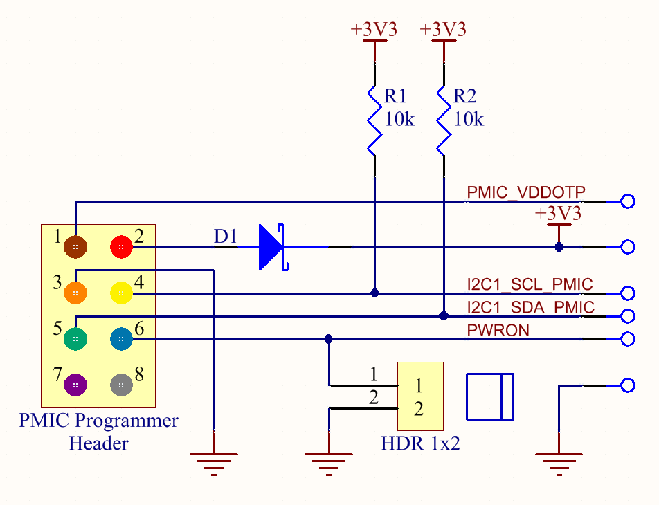
Important notes:
- Remove resistor bypassing I2C1 with PMIC I2C (Remove R238 and R247)
- Place pullup resistors to I2C signals
- PMIC VDDOTP voltage should be disconnected for Try-Before-Buy mode (just to be safe)
- +3V3 power voltage is protected from backward leaking from board to programmer (we used a standard 1A Schottky diode)
| Position - Ribbon color | Programmer header | OpenRex | |
| Pin 1 - brown | VPGM | PMIC_VDDOTP (for TBB NC) | |
| Pin 2 - red | V3V3 ->diode-> | +3V3 (R226-pin 2) | |
| Pin 3 - orange | GROUND | GND (U23-pin 2) | |
| Pin 4 - yellow | SCL | I2C1_SCL_PMIC (big VIA) | |
| Pin 5 - green | SDA | I2C1_SDA_PMIC (big VIA) | |
| Pin 6 - blue | PWRON | PWRON (big VIA) | |
| Pin 7 - violet | GPIO1 | NC | |
| Pin 8 - grey | GPIO2 | NC |
Try-before-buy programming procedure
For temporary programming we will use slightly updated process as we use with development board:1. Open PF_Series_HID.application and connect PF Series Programmer with PC using USB Mini cable
2. Connect 5V input voltage to the OpenRex board
3. Plug the connector with soldered wires into the PMIC programmer
4. Enable Target and scan for the devices in the application. At this point you should see these messages in the log area:
Target = PF-Programmer
Device Found
3.3V Supply Enabled
Target Enabled
Device with address [0x08] available
5. Go to script Editor tab and Copy there our Try before buy script. Run the script
6. Fit link between PWRON and GND
7. Send command through Script editor (clear existing first) to put PWRON high (send PWRON:HIGH)
8. Remove programming header
9. Release PWRON signal (remove the link)
10. If everything else was setup correctly u-boot will now appear on the serial console
One-time-programming procedure
Steps for permanent setup of PMIC fuses are exactly the same as for TBB mode just in the point 5 load One time programming script instead. Be sure VDDOTP voltage is connected to the board.Caution: Do not try to program fuses your OpenRex board - it has been already programmed!
Scripts
Go to projects GitHub page for all scripts and changes which have been made.Try Before buy script
///---------------------------------------------------------------------------
// OpenRex - Sample Try-Before-Buy Configuration
// Set VDDOTP = 0 V, PWRON = HIGH, LICELL not used, VIN = 4.2 V,  VDDIO = 3.3 V
//---------------------------------------------------------------------------
WRITE_I2C:7F:01 // Access PF0100 EXT Page1
//[Extended Page 1 Registers: 0xA0 - 0xAF] ----------------------------------
WRITE_I2C:A0:2B // Sw1AB Voltage = 1.375 V
WRITE_I2C:A1:02 // Sw1AB Sequence = 2
WRITE_I2C:A2:05 // Sw1AB Freq = 2 MHZ, Mode = Single phase
WRITE_I2C:A8:2B // Sw1c Voltage = 1.375 V
WRITE_I2C:A9:03 // Sw1c Sequence = 3
WRITE_I2C:AA:01 // Sw1c Freq = 2.0 MHZ
WRITE_I2C:AC:72 // Sw2 Voltage = 3.30 V
WRITE_I2C:AD:06 // Sw2 Sequence = 6
WRITE_I2C:AE:01 // Sw2 Freq = 2 MHZ
//[Extended Page 1 Registers: 0xB0 - 0xBF] ----------------------------------
WRITE_I2C:B0:2C // Sw3A Voltage = 1.500 V
WRITE_I2C:B1:04 // Sw3A Sequence = 4
WRITE_I2C:B2:05 // Sw3A Freq = 2 MHZ, Mode = Single phase
WRITE_I2C:B4:2C // Sw3B Voltage = 1.500 V
WRITE_I2C:B5:04 // Sw3B Sequence = 4
WRITE_I2C:B6:01 // Sw3B Freq = 2 MHZ
WRITE_I2C:B8:38 // Sw4 Voltage = 1.350 V
WRITE_I2C:B9:05 // Sw4 Sequence = 5
WRITE_I2C:BA:11 // Sw4 VTT Mode enable, Freq = 2 MHZ
WRITE_I2C:BC:00 // Swbst Voltage = 5.0 V
WRITE_I2C:BD:08 // Swbst Sequence = 8
//[Extended Page 1 Registers: 0xC0 - 0xCF] ----------------------------------
WRITE_I2C:C0:06 // Vsnvs Voltage = 3.0 V
WRITE_I2C:C4:03 // VREF DDR Sequence = 3
WRITE_I2C:C8:0E // Vgen1 Voltage = 1.5 V
WRITE_I2C:C9:0B // Vgen1 Sequence = 11
WRITE_I2C:CC:08 // Vgen2 Voltage = 1.2 V
WRITE_I2C:CD:09 // Vgen2 Sequence = 9
//[Extended Page 1 Registers: 0xD0 - 0xDF] ----------------------------------
WRITE_I2C:D0:00 // Vgen3 Voltage = 1.8 V
WRITE_I2C:D1:0A // Vgen3 Sequence = 10
WRITE_I2C:D4:07 // Vgen4 Voltage = 2.5 V
WRITE_I2C:D5:07 // Vgen4 Sequence = 7
WRITE_I2C:D8:0F // Vgen5 Voltage = 3.3 V
WRITE_I2C:D9:0C // Vgen5 Sequence = 12
WRITE_I2C:DC:0C // Vgen6 Voltage = 3.0 V
WRITE_I2C:DD:01 // Vgen6 Sequence = 1
//[Extended Page 1 Registers: 0xE0 - 0xEF] ----------------------------------
WRITE_I2C:E0:0F // Power-up DVS = 1.5625 mV/us, SeqCLK = 4 ms, PWRON config = 0
WRITE_I2C:E1:0F // Power-up DVS = 1.5625 mV/us, SeqCLK = 4 ms, PWRON config = 0
WRITE_I2C:E2:0F // Power-up DVS = 1.5625 mV/us, SeqCLK = 4 ms, PWRON config = 0
WRITE_I2C:E8:01 // Fault Mode = Enabled
//[Extended Page 1 Registers: 0xF0 - 0xFF] ----------------------------------
WRITE_I2C:FF:08 // I2C Device Address = 0x08
//===========================================================================
// TRY-BEFORE-BUY COMMANDS FOLLOW
//===========================================================================
WRITE_I2C:E4:80 // TBB POR=1 (This Enables TBB Mode)
//---------------------------------------------------------------------------
PWRON:LOW // PWRON LOW
DELAY:500
// !!!IMPORTANT!!!
// Unplug programming header and AFTER that send PWRON HIGH
One Time Programming script
///---------------------------------------------------------------------------
// OpenRex - Sample Try-Before-Buy Configuration
// Set VDDOTP = 0 V, PWRON = HIGH, LICELL not used, VIN = 4.2 V,  VDDIO = 3.3 V
//---------------------------------------------------------------------------
WRITE_I2C:7F:01 // Access PF0100 EXT Page1
//[Extended Page 1 Registers: 0xA0 - 0xAF] ----------------------------------
WRITE_I2C:A0:2B // Sw1AB Voltage = 1.375 V
WRITE_I2C:A1:02 // Sw1AB Sequence = 2
WRITE_I2C:A2:05 // Sw1AB Freq = 2 MHZ, Mode = Single phase
WRITE_I2C:A8:2B // Sw1c Voltage = 1.375 V
WRITE_I2C:A9:03 // Sw1c Sequence = 3
WRITE_I2C:AA:01 // Sw1c Freq = 2.0 MHZ
WRITE_I2C:AC:72 // Sw2 Voltage = 3.30 V
WRITE_I2C:AD:06 // Sw2 Sequence = 6
WRITE_I2C:AE:01 // Sw2 Freq = 2 MHZ
//[Extended Page 1 Registers: 0xB0 - 0xBF] ----------------------------------
WRITE_I2C:B0:2C // Sw3A Voltage = 1.500 V
WRITE_I2C:B1:04 // Sw3A Sequence = 4
WRITE_I2C:B2:05 // Sw3A Freq = 2 MHZ, Mode = Single phase
WRITE_I2C:B4:2C // Sw3B Voltage = 1.500 V
WRITE_I2C:B5:04 // Sw3B Sequence = 4
WRITE_I2C:B6:01 // Sw3B Freq = 2 MHZ
WRITE_I2C:B8:38 // Sw4 Voltage = 1.350 V
WRITE_I2C:B9:05 // Sw4 Sequence = 5
WRITE_I2C:BA:11 // Sw4 VTT Mode enable, Freq = 2 MHZ
WRITE_I2C:BC:00 // Swbst Voltage = 5.0 V
WRITE_I2C:BD:08 // Swbst Sequence = 8
//[Extended Page 1 Registers: 0xC0 - 0xCF] ----------------------------------
WRITE_I2C:C0:06 // Vsnvs Voltage = 3.0 V
WRITE_I2C:C4:03 // VREF DDR Sequence = 3
WRITE_I2C:C8:0E // Vgen1 Voltage = 1.5 V
WRITE_I2C:C9:0B // Vgen1 Sequence = 11
WRITE_I2C:CC:08 // Vgen2 Voltage = 1.2 V
WRITE_I2C:CD:09 // Vgen2 Sequence = 9
//[Extended Page 1 Registers: 0xD0 - 0xDF] ----------------------------------
WRITE_I2C:D0:00 // Vgen3 Voltage = 1.8 V
WRITE_I2C:D1:0A // Vgen3 Sequence = 10
WRITE_I2C:D4:07 // Vgen4 Voltage = 2.5 V
WRITE_I2C:D5:07 // Vgen4 Sequence = 7
WRITE_I2C:D8:0F // Vgen5 Voltage = 3.3 V
WRITE_I2C:D9:0C // Vgen5 Sequence = 12
WRITE_I2C:DC:0C // Vgen6 Voltage = 3.0 V
WRITE_I2C:DD:01 // Vgen6 Sequence = 1
//[Extended Page 1 Registers: 0xE0 - 0xEF] ----------------------------------
WRITE_I2C:E0:0F // Power-up DVS = 1.5625 mV/us, SeqCLK = 4 ms, PWRON config = 0
WRITE_I2C:E1:0F // Power-up DVS = 1.5625 mV/us, SeqCLK = 4 ms, PWRON config = 0
WRITE_I2C:E2:0F // Power-up DVS = 1.5625 mV/us, SeqCLK = 4 ms, PWRON config = 0
WRITE_I2C:E8:01 // Fault Mode = Enabled
//[Extended Page 1 Registers: 0xF0 - 0xFF] ----------------------------------
WRITE_I2C:FF:08 // I2C Device Address = 0x08
//===========================================================================
// ONE TIME PROGRAMMING COMMANDS FOLLOW
//===========================================================================
WRITE_I2C:E4:02 // FUSE POR=1 (This Enables OTP Programming)
WRITE_I2C:E5:02 // FUSE POR=1 (This Enables OTP Programming)
WRITE_I2C:E6:02 // FUSE POR=1 (This Enables OTP Programming)
//-----------------------------------------------------------------------------------
WRITE_I2C:F0:1F // Enable ECC for fuse banks 1 to 5 by writing to OTP EN ECC0 register
WRITE_I2C:F1:1F // Enable ECC for fuse banks 6 to 10 by writing to OTP EN ECC1 register
WRITE_I2C:7F:02 // Access PF0100 EXT Page2
WRITE_I2C:D0:1F // Set Auto ECC for fuse banks 1 to 5 by writing to OTP AUTO ECC0 register
WRITE_I2C:D1:1F // Set Auto ECC for fuse banks 6 to 10 by writing to OTP AUTO ECC1 register
//-----------------------------------------------------------------------------------
WRITE_I2C:F1:00 // Reset Bank 1 ANTIFUSE_RW and ANTIFUSE_BYPASS bits
WRITE_I2C:F2:00 // Reset Bank 2 ANTIFUSE_RW and ANTIFUSE_BYPASS bits
WRITE_I2C:F3:00 // Reset Bank 3 ANTIFUSE_RW and ANTIFUSE_BYPASS bits
WRITE_I2C:F4:00 // Reset Bank 4 ANTIFUSE_RW and ANTIFUSE_BYPASS bits
WRITE_I2C:F5:00 // Reset Bank 5 ANTIFUSE_RW and ANTIFUSE_BYPASS bits
WRITE_I2C:F6:00 // Reset Bank 6 ANTIFUSE_RW and ANTIFUSE_BYPASS bits
WRITE_I2C:F7:00 // Reset Bank 7 ANTIFUSE_RW and ANTIFUSE_BYPASS bits
WRITE_I2C:F8:00 // Reset Bank 8 ANTIFUSE_RW and ANTIFUSE_BYPASS bits
WRITE_I2C:F9:00 // Reset Bank 9 ANTIFUSE_RW and ANTIFUSE_BYPASS bits
WRITE_I2C:FA:00 // Reset Bank 10 ANTIFUSE_RW and ANTIFUSE_BYPASS bits
//-----------------------------------------------------------------------------------
VPGM:ON // Turn ON 8V SWBST
//VPGM:DOWN:n
//VPGM:UP:n
DELAY:500 // Adds 500msec delay to allow VPGM time to ramp up
//-----------------------------------------------------------------------------------
// PF0100 OTP MANUAL-PROGRAMMING (BANK 1 thru 10)
//-----------------------------------------------------------------------------------
// BANK 1
//-----------------------------------------------------------------------------------
WRITE_I2C:F1:03 // Set Bank 1 ANTIFUSE_RW and ANTIFUSE_BYPASS bits
WRITE_I2C:F1:0B // Set Bank 1 ANTIFUSE_EN
DELAY:10 // Allow time for bank programming to complete
WRITE_I2C:F1:03 // Reset Bank 1 ANTIFUSE_EN
WRITE_I2C:F1:00 // Reset Bank 1 ANTIFUSE_RW and ANTIFUSE_BYPASS bits
//-----------------------------------------------------------------------------------
// BANK 2
//-----------------------------------------------------------------------------------
WRITE_I2C:F2:03 // Set Bank 2 ANTIFUSE_RW and ANTIFUSE_BYPASS bits
WRITE_I2C:F2:0B // Set Bank 2 ANTIFUSE_EN
DELAY:10 // Allow time for bank programming to complete
WRITE_I2C:F2:03 // Reset Bank 2 ANTIFUSE_EN
WRITE_I2C:F2:00 // Reset Bank 2 ANTIFUSE_RW and ANTIFUSE_BYPASS bits
//-----------------------------------------------------------------------------------
// BANK 3
//-----------------------------------------------------------------------------------
WRITE_I2C:F3:03 // Set Bank 3 ANTIFUSE_RW and ANTIFUSE_BYPASS bits
WRITE_I2C:F3:0B // Set Bank 3 ANTIFUSE_EN
DELAY:10 // Allow time for bank programming to complete
WRITE_I2C:F3:03 // Reset Bank 3 ANTIFUSE_EN
WRITE_I2C:F3:00 // Reset Bank 3 ANTIFUSE_RW and ANTIFUSE_BYPASS bits
//-----------------------------------------------------------------------------------
// BANK 4
//-----------------------------------------------------------------------------------
WRITE_I2C:F4:03 // Set Bank 4 ANTIFUSE_RW and ANTIFUSE_BYPASS bits
WRITE_I2C:F4:0B // Set Bank 4 ANTIFUSE_EN
DELAY:10 // Allow time for bank programming to complete
WRITE_I2C:F4:03 // Reset Bank 4 ANTIFUSE_EN
WRITE_I2C:F4:00 // Reset Bank 4 ANTIFUSE_RW and ANTIFUSE_BYPASS bits
//-----------------------------------------------------------------------------------
// BANK 5
//-----------------------------------------------------------------------------------
WRITE_I2C:F5:03 // Set Bank 5 ANTIFUSE_RW and ANTIFUSE_BYPASS bits
WRITE_I2C:F5:0B // Set Bank 5 ANTIFUSE_EN
DELAY:10 // Allow time for bank programming to complete
WRITE_I2C:F5:03 // Reset Bank 5 ANTIFUSE_EN
WRITE_I2C:F5:00 // Reset Bank 5 ANTIFUSE_RW and ANTIFUSE_BYPASS bits
//-----------------------------------------------------------------------------------
// BANK 6
//-----------------------------------------------------------------------------------
WRITE_I2C:F6:03 // Set Bank 6 ANTIFUSE_RW and ANTIFUSE_BYPASS bits
WRITE_I2C:F6:0B // Set Bank 6 ANTIFUSE_EN
DELAY:10 // Allow time for bank programming to complete
WRITE_I2C:F6:03 // Reset Bank 6 ANTIFUSE_EN
WRITE_I2C:F6:00 // Reset Bank 6 ANTIFUSE_RW and ANTIFUSE_BYPASS bits
//-----------------------------------------------------------------------------------
// BANK 7
//-----------------------------------------------------------------------------------
WRITE_I2C:F7:03 // Set Bank 7 ANTIFUSE_RW and ANTIFUSE_BYPASS bits
WRITE_I2C:F7:0B // Set Bank 7 ANTIFUSE_EN
DELAY:10 // Allow time for bank programming to complete
WRITE_I2C:F7:03 // Reset Bank 7 ANTIFUSE_EN
WRITE_I2C:F7:00 // Reset Bank 7 ANTIFUSE_RW and ANTIFUSE_BYPASS bits
//-----------------------------------------------------------------------------------
// BANK 8
//-----------------------------------------------------------------------------------
WRITE_I2C:F8:03 // Set Bank 8 ANTIFUSE_RW and ANTIFUSE_BYPASS bits
WRITE_I2C:F8:0B // Set Bank 8 ANTIFUSE_EN
DELAY:10 // Allow time for bank programming to complete
WRITE_I2C:F8:03 // Reset Bank 8 ANTIFUSE_EN
WRITE_I2C:F8:00 // Reset Bank 8 ANTIFUSE_RW and ANTIFUSE_BYPASS bits
//-----------------------------------------------------------------------------------
// BANK 9
//-----------------------------------------------------------------------------------
WRITE_I2C:F9:03 // Set Bank 9 ANTIFUSE_RW and ANTIFUSE_BYPASS bits
WRITE_I2C:F9:0B // Set Bank 9 ANTIFUSE_EN
DELAY:10 // Allow time for bank programming to complete
WRITE_I2C:F9:03 // Reset Bank 9 ANTIFUSE_EN
WRITE_I2C:F9:00 // Reset Bank 9 ANTIFUSE_RW and ANTIFUSE_BYPASS bits
//-----------------------------------------------------------------------------------
// BANK 10
//-----------------------------------------------------------------------------------
WRITE_I2C:FA:03 // Set Bank 10 ANTIFUSE_RW and ANTIFUSE_BYPASS bits
WRITE_I2C:FA:0B // Set Bank 10 ANTIFUSE_EN
DELAY:10 // Allow time for bank programming to complete
WRITE_I2C:FA:03 // Reset Bank 10 ANTIFUSE_EN
WRITE_I2C:FA:00 // Reset Bank 10 ANTIFUSE_RW and ANTIFUSE_BYPASS bits
//-----------------------------------------------------------------------------------
WRITE_I2C:D0:00 // Clear
WRITE_I2C:D1:00 // Clear
//-----------------------------------------------------------------------------------
VPGM:OFF // Turn off 8V SWBST
DELAY:500 // Adds delay to allow VPGM to bleed off
PWRON:LOW // PWRON LOW to reload new OTP data
DELAY:500
// !!!IMPORTANT!!!
// Unplug programming header and AFTER that send PWRON HIGH